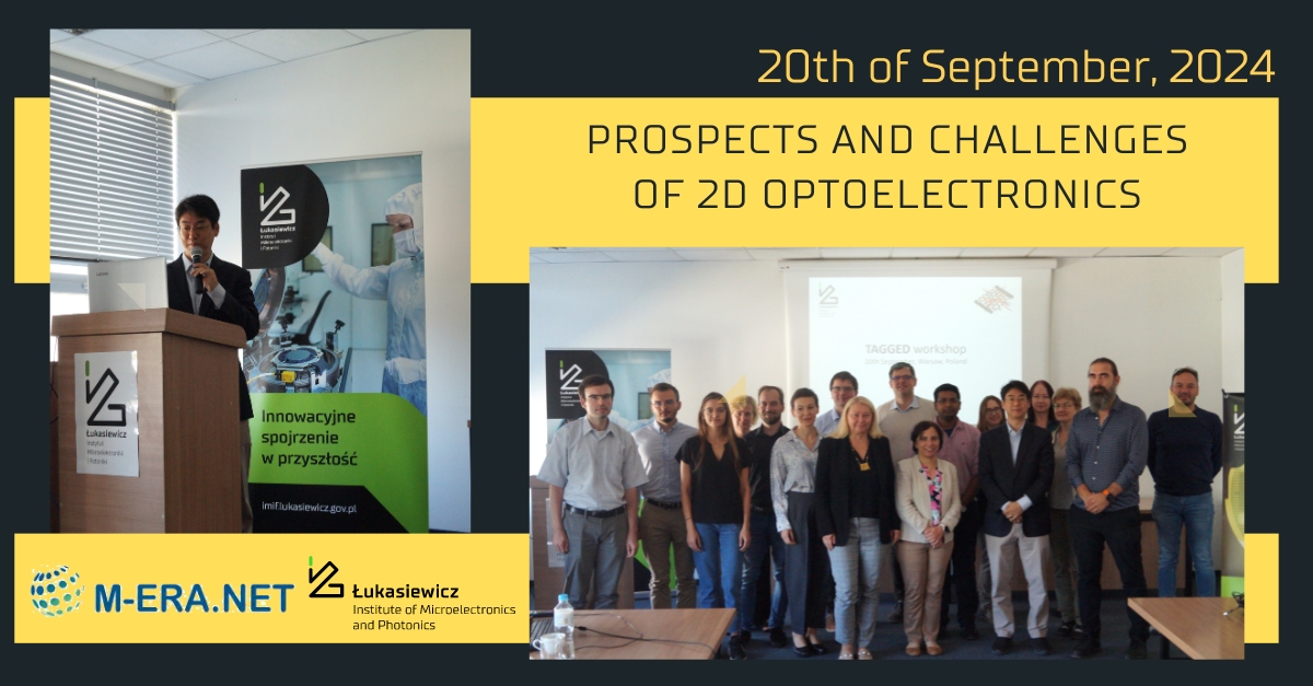
On September 20th, a workshop on 2D optoelectronics entitled “Prospects and Challenges of 2D Optoelectronics” was held at our institute.
The event, organized by the Smart Materials Research Group was preceded by a meeting of the TAGGED project, ” Research, Development and characterization of a TunAble Graphene liGht Emitting hybrid MOEMS Device,” realized under the M-Era.Net call 2020 programme. The project is being conducted by a consortium that consists of Fraunhofer ENAS (leader), the J. Heyrovsky Institute of Physical Chemistry, TU Bergakademie Freiberg, the Institute of Electronic and Sensor Materials, and Łukasiewicz – Institute of Microelectronics and Photonics.
During the TAGGED workshop led by Dr. hab. Anna Kozłowska, attendees had the opportunity to listen to five presentations. Three of them were invited lectures:
- “Ultrafast Graphene Light Source” presented by Prof. Young Duck Kim from Kyung Hee University, Seoul, Republic of Korea;
- Dr. Sacha Hermann from Fraunhofer ENAS (Germany) joined us online and discussed talked about the Integration of low-dimensional Nanomaterials – progress on wafer level technologies;
- Dr. Paweł Michałowski from our institute presented the results of 2D material characterization using Secondary Ion Mass Spectrometry.
The TAGGED project leader, Dr. Nooshin Saedi from Fraunhofer ENAS, delivered a lecture entitled “ TAGGED: A MEMS-driven platform for tunable 2D light sources.”
The lecture session concluded with a talk by Dr. Martin Kalbáč from the J. Heyrovsky Institute of Physical Chemistry in Prague, entitled “2D Materials for Application in Devices.”
After the lectures, guests visited the Smart Materials Research Group laboratories and the Characterization of Materials and Devices Research Group laboratories.
The TAGGED project is part of the M-Era Net 2020 call, and the part of the project carried out in Poland is funded by the National Science Centre (NCN), project number UMO-2020/02/Y/ST5/00105.