Devices based on ultrawide bandgap semiconductors (with energy bandgaps over 4 eV), such as gallium oxide, can work at much higher voltages than devices based on silicon since with the increase in the width of the energy gap, the value of the critical electric field also increases. Moreover, the ultra-wide bandgap means that these materials can theoretically operate at much higher temperatures.
In order to obtain higher breakdown voltage for the same layer thickness and doping as for other materials, it is possible to use thinner or more heavily doped layers. This will reduce resistance and thus losses. It is also worth mentioning that the thinner the layer, the shorter the growth process and the lower the price of the epitaxial structure (less reagent consumption and more structures can be made at the same time).
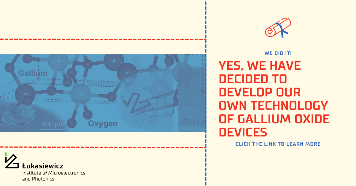
Gallium oxide, a member of UWBG semiconductors, can also be used as the material for the detection of deep ultraviolet radiation, for example, to detect the radiation emitted by germicidal lamps (with a wavelength of 254 nm), which kills viruses and destroys DNA, widely used for disinfection.
Other advantages of gallium oxide, include the possibility to obtain larger wafers – this means that technologies can be easily scaled and introduced to technological production lines, larger wafers mean higher yield and lower cost of manufacturing devices.