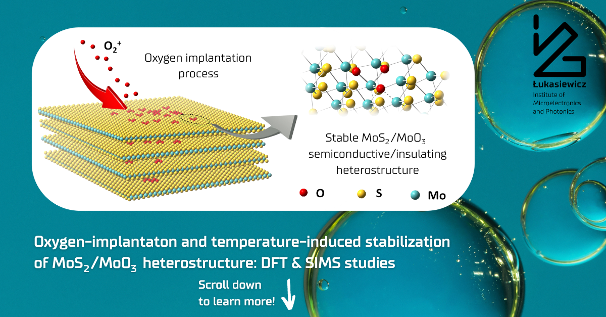
A new heterostructure has been created! 2D MoS2 is a semiconductor and what that means is that its properties can be controlled and its conductivity can be induced. MoS2 has the advantages of abundant reserves, low cost, favorable biocompatibility, good mechanical properties, and high chemical stability. It has also unique optical catalytical, and electrical properties. However, 2D MoS2 can gain totally different properties and our researchers have shown how exactly this is possible!
They have discovered that by implanting oxygen atoms into 2D MoS2, they can create a new structure called MoS2/MoO3 heterostructure, which boasts promising properties.
(MoS2 has been implanted with oxygen, but it wasn’t so obvious that the oxygen would stay inside and bond with the molybdenum there to form MoO3.)
Did you know that this new structure allows for different combinations of properties and opens up new possibilities for practical applications in mechanics, electronics, optoelectronics, and thermoelectronics?
To study this new material, the researchers have used a technique called SIMS for precise analysis of the chemical composition of the sample layer by layer. This technique allows you to study 2D materials with subnanometer resolution and excellent sensitivity! They have also used the DFT technique which has shown the consequences of the formation of MoO3 in the MoS2 layer for shifting the bandgap, but also allowed to estimate the stability of the structure.
One of the exciting potential applications for this material is in photovoltaics, where it shows promise for harnessing solar energy. The band gap value, an important factor for photovoltaic applications, can be estimated using the DFT technique about which Sylwia Kozdra, PhD, specialized at the Hylleraas Center for Quantum Molecular Sciences, University of Oslo, known for its experience in quantum-chemical calculations.
More: sciencedirect.com


