Today, our master chef recommends a typical American Breakfast – cinnamon waffles. Please don’t confuse it with silicon wafers. That’s what our two brave conquerors of the world would eat in the morning when staying in the US where they were taking part in the Nanotech’22 conference that was a part of TechConnect World Innovation Conference & Expo (which by the way, celebrated its 25th anniversary).
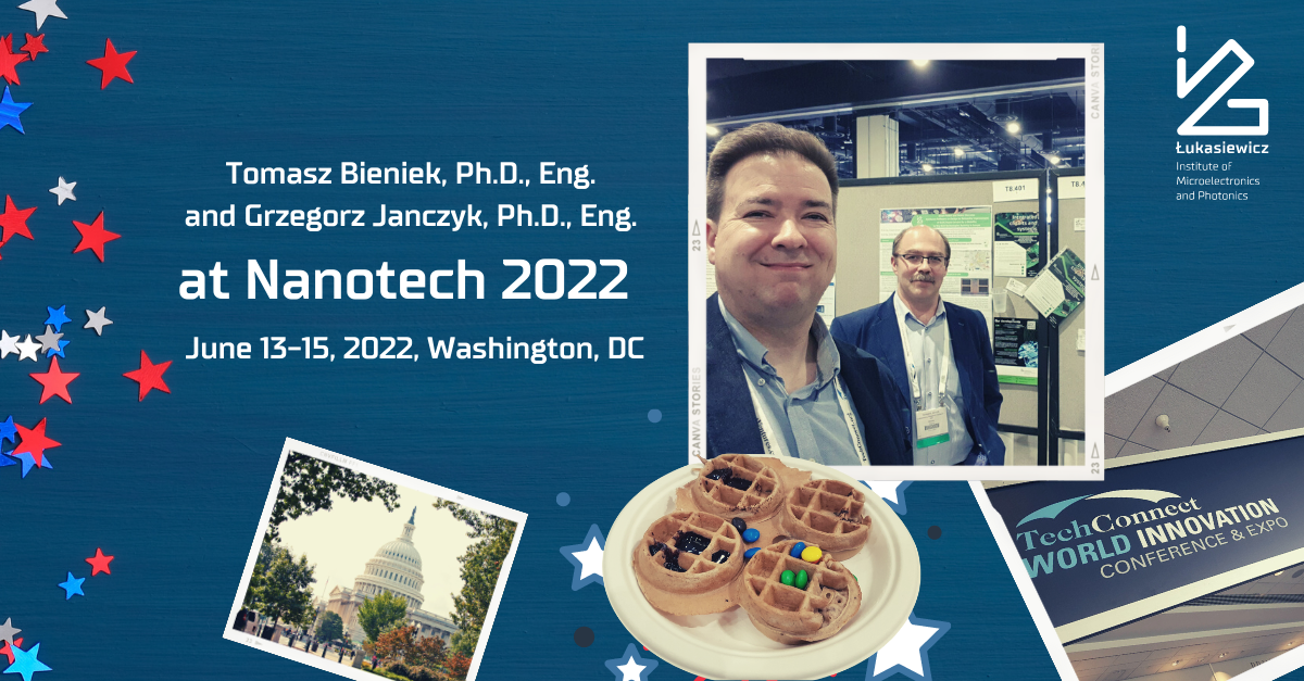
If you’re still not sure who we’re talking about… it’s all about Tomasz Bieniek, Ph.D., and Grzegorz Janczyk, Ph.D. who have taken part in the aforementioned conference for the last 10 years.
Finally, after a 2-years pandemic break (COVID) they were back there again. Our research conquerors had a chance to present 2 articles summarizing two big European H2020 projects important for European microelectronics: REACTION project and R3-PowerUP project – both led by STMicroelectronics and both focused respectively on powerelectronics developed on Silicon (R3-PowerUP) and Silicon Carbide (REACTION) technology.
The REACTION project was launched in 2018 to push throughout the first European 200mm (8”) SiC Pilot Line – and first in the world! Some of the 27 partners, including our Institute, are responsible for the development of DC/DC modules up to 20kW as one of the REACTION project demonstrators. The solution being developed now has the potential for numerous applications from energy storage equipment up to electric vehicle charging stations, power management, green energy management, etc… The REACTION Polish cluster with STMicroelectronics and some other project partners is also responsible for SiC Power MOSFET gate driver development and its application for a power management module development with strong focus commercialization scenario.
The R3-PowerUP project is focused on 90nm (BCD9) and 110nm (BCD10) feature size Bipolar-CMOS-DMOS (BCD) processes. According to the increasing market demand for cheap electronics and components, BCD9 and BCD10 have been selected for migration from 200mm Si substrates (the technology now available and running) to 300mm diameter substrates in order to reduce the final price of the single-chip and additionally have it fabricated in the European Pilot Line Facility for Smart Power technology in Agrate, Italy. The migration to 300mm wafer size involves both power discrete and advanced smart power/logic/PCM (non-volatile memories). The R3PowerUP Polish cluster with STMicroelectronics and some other project partners is responsible for one of the project demonstrator – the BCD technology-based BLDC driver for synchronous DC motors commutated electronically.