On November 15-18, we will be at the Electronica fair in Munich. Previously, we have written about ASIC and MEMS – the technologies that we’re going to present to you at the aforementioned trade fair. Now it’s time for another interesting abbreviation – GaN, i.e. gallium nitride. GaN-based devices, sensors, thin-film structures, and porous materials Research Group, led by dr hab. Anna Szerling, will have the pleasure of demonstrating the following subjects during the upcoming event:
1. GaN transistors,
2. functional coatings, for instance for optical sensors or black absorbing coatings,
3. diffractive optical elements,
4. conducting films for ohmic contacts to optoelectronic devices
5. photolithography masks.
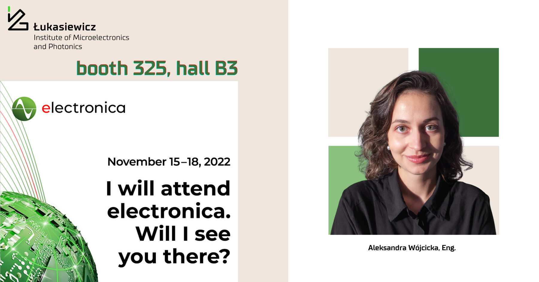
The Group offers specialized research and development services in the field of GaN-based microelectronic devices, thin-film structures, sensors, porous materials, and diffractive optical elements. Do you want to know more? Aleksandra Wójcicka, Eng. will be waiting for you at stand no. 325 in hall B3 to answer any questions you might have.