Oferta własności intelektualnej
Poniżej znajduje się lista praw własności przemysłowej obejmująca technologie wypracowane w Łukasiewicz – IMiF.
Zainteresowanych zakupem lub licencjonowaniem praw do poniższych rozwiązań zapraszamy do kontaktu: komercjalizacja@imif.lukasiewicz.gov.pl
Patent information
Title: Method of silvering surfaces, especially aluminium surfaces
(PL: Sposób srebrzenia powierzchni, zwłaszcza aluminium)
Patent number: EP2447313
Application number: EP11180709
Application date: 09.09.2011
Inventors: Marian Teodorczyk, Jeremiasz Olgierd, Mateusz Jarosz, Anna Młożniak, Małgorzata Jakubowska
Owner: Łukasiewicz – Institute of Microelectronic and Photonics
Jurisdictions: France, Great Britain, Germany, Poland.
Espacenet: https://worldwide.espacenet.com/patent/search/family/044799628/publication/EP2447313B1?q=EP2447313
The technology in a nutshell
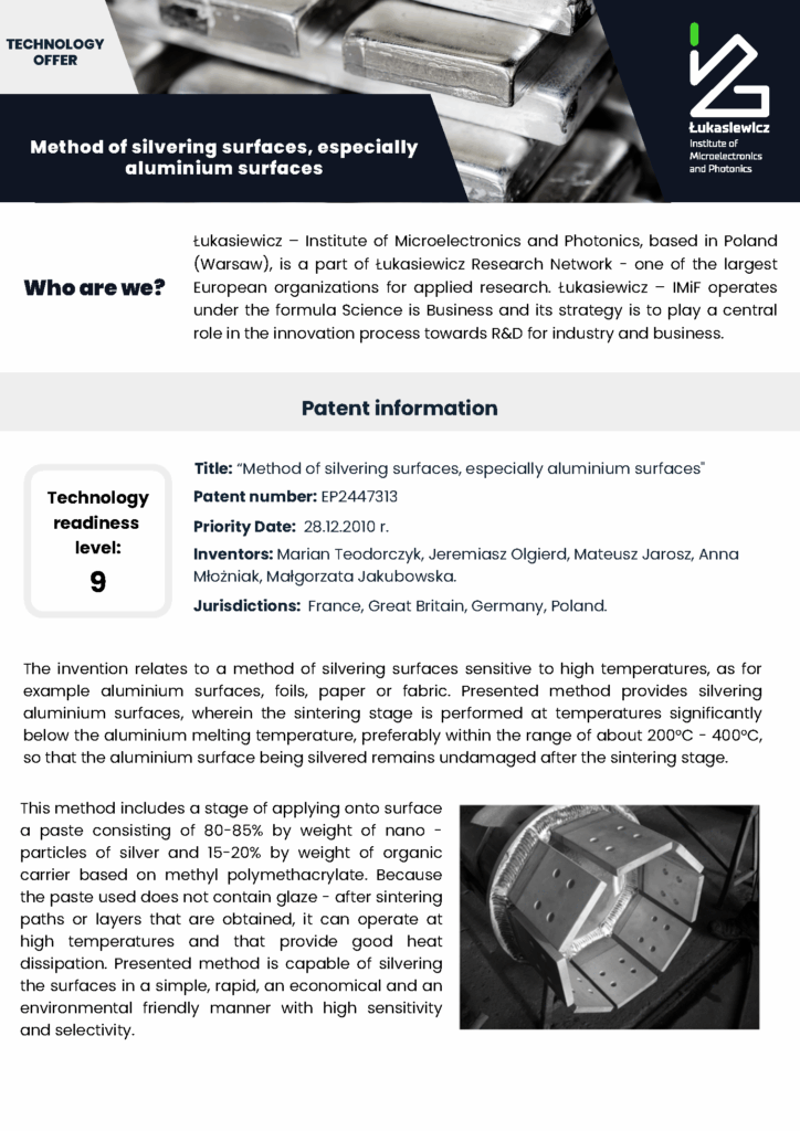
The invention relates to a method of silvering surfaces sensitive to high temperatures, as for example aluminium surfaces, foils, paper or fabric.
Presented method provides silvering aluminium surfaces, wherein the sintering stage is performed at temperatures significantly below the aluminium melting temperature, preferably within the range of about 200°C – 400°C, so that the aluminium surface being silvered remains undamaged after the sintering stage.
Our method is capable of silvering the surfaces in a simple, rapid, an economical and an environmental friendly manner with high sensitivity and selectivity.
A photonic crystal fibre for transferring radially polarised light beam and a method of manufacturing such a fibre
EP3073300, Pat.226041
Patent information
Title: A photonic crystal fibre for transferring radially polarised light beam and a method of manufacturing such a fibre
(PL: Światłowód fotoniczny do przenoszenia wiązki światła spolaryzowanej radialnie i sposób wytwarzania takiego światłowodu)
Patent number: EP3073300, Pat.226041
Application number: EP15180047, P.411696
Application date: 06.08.2015 (EP), 25.03.2015 (PL)
Inventors: Ryszard Buczyński, Tomasz Stefaniuk, Jacek Pniewski, Dariusz Pysz, Grzegorz Stępniewski, Ryszard Stępień
Owner: Łukasiewicz – Institute of Microelectronic and Photonics
Jurisdictions: Germany, France, Great Britain, Poland
Espacenet: https://worldwide.espacenet.com/patent/search/family/054251918/publication/EP3073300B1?q=EP3073300b1
The technology in a nutshell
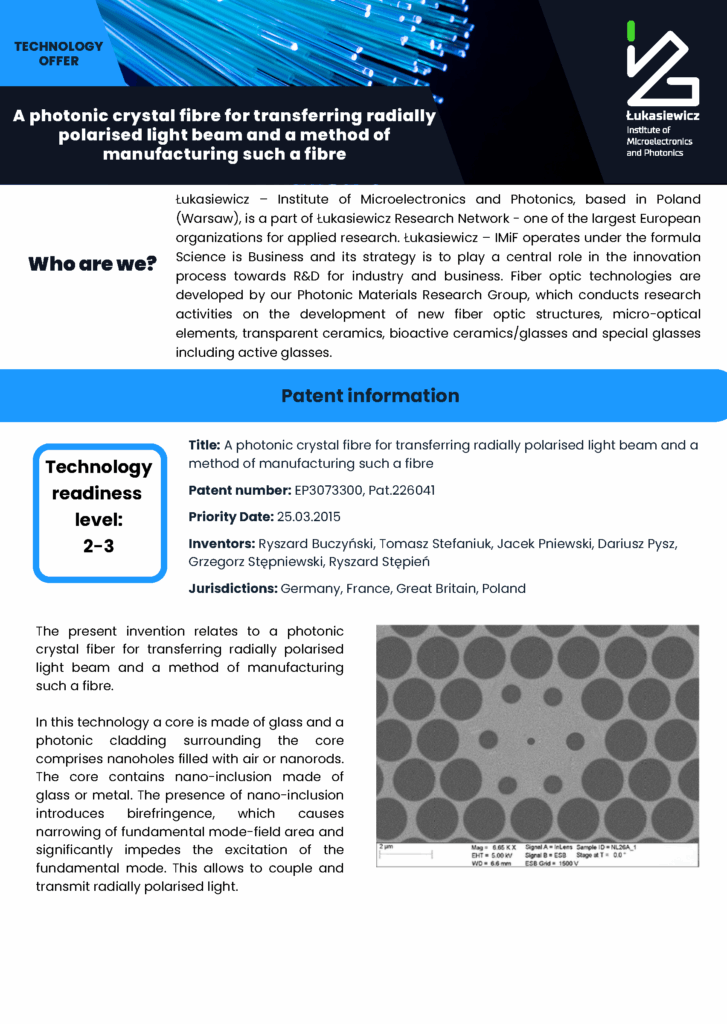
The present invention relates to a photonic crystal fiber for transferring radially polarised light beam and a method of manufacturing such a fibre.
In this technology a core is made of glass and a photonic cladding surrounding the core comprises nanoholes filled with air or nanorods. The core contains nano-inclusion made of glass or metal. The presence of nano-inclusion introduces birefringence, which causes narrowing of fundamental mode-field area and significantly impedes the excitation of the fundamental mode. This allows to couple and transmit radially polarised light.
Patent information
Title: Diagnostic insert for shoes
(PL: Wkładka diagnostyczna)
Patent number: Pat.225306
Application number: P.402006
Application date: 11.12.2012
Inventors: Ewa Klimiec, Wiesław Zaraska, Jacek Piekarski, Krzysztof Zaraska,Andrzej Cichocki, Grzegorz Czyrnek, Barbara Jasiewicz
Owner: Łukasiewicz – IMiF, Uniwersytecki Szpital Ortopedyczno – Rehabilitacyjny w Zakopanem
Jurisdictions: Poland
The technology in a nutshell
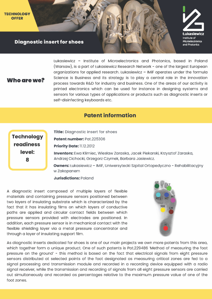
Our diagnostic insert is composed of multiple layers of flexible materials and containing pressure sensors positioned between two layers of insulating substrate which is characterized by the fact that it has insulating films on which layers of conductive paths are applied and circular contact fields between which pressure sensors provided with electrodes are positioned. In addition, each pressure sensor is in mechanical contact with the flexible shielding layer via a metal pressure concentrator and through a layer of insulating support film.
Our insert, when placed in footwear and connected to a portable miniature measuring system, allows dynamic testing of foot pressure distribution under any conditions, i.e. during running, walking or jumping.
The low cost of manufacturing our insert means that it can be made in many sizes and large quantities, and even produced as a single-use product, which will ensure patient comfort and promote hygiene.
Patent information
Title: Method of measuring the foot pressure on the ground
(PL: Sposób pomiaru nacisku stopy na podłoże)
Patent number: Pat.229486
Application number: P.404016
Application date: 22.05.2013
Inventors: Ewa Klimiec, Wiesław Zaraska, Jacek Piekarski, Andrzej Cichocki, Barbara Jasiewicz, Maciej Tęsiorowski
Owner: Łukasiewicz – IMiF, Uniwersytecki Szpital Ortopedyczno – Rehabilitacyjny w Zakopanem
Jurisdictions: Poland
Espacenet:
The technology in a nutshell
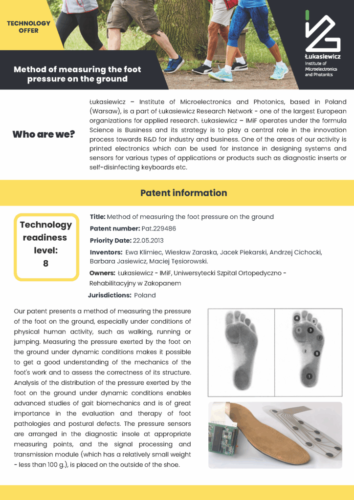
Our patent presents a method of measuring the pressure of the foot on the ground, especially under conditions of physical human activity, such as walking, running or jumping. Measuring the pressure exerted by the foot on the ground under dynamic conditions makes it possible to get a good understanding of the mechanics of the foot’s work and to assess the correctness of its structure.
Presented device for measuring the distribution of pressure exerted by the feet used in the rehabilitation process allows for an overall assessment of a person’s movement capabilities, as there is a correlation between foot fitness and defects in the knees, hips and spine.
The main advantage of a system incorporating the measuring insert according to the invention is the ability to conduct tests in natural non-clinical settings, such as during home activities, exercise and field stays. The low cost of manufacturing our insert means that it can be made in many sizes and large quantities
Patent information
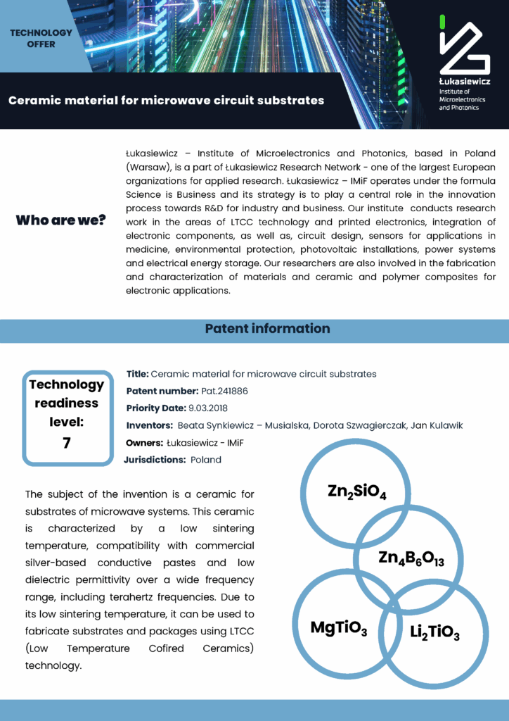
Title: Ceramic material for microwave circuit substrates
(PL: Ceramika na podłoża układów mikrofalowych)
Patent number: Pat.241886
Application number: P.424832
Application date: 9.03.2018
Inventors: : Beata Synkiewicz – Musialska, Dorota Szwagierczak, Jan Kulawik
Owner: Łukasiewicz – IMiF
Jurisdictions: Poland
The technology in a nutshell
The subject of the invention is a ceramic for substrates of microwave systems. This ceramic is characterized by a low sintering temperature, compatibility with commercial silver-based conductive pastes and low dielectric permittivity over a wide frequency range, including terahertz frequencies. Due to its low sintering temperature, it can be used to fabricate substrates and packages using LTCC (Low Temperature Cofired Ceramics) technology.
Ceramic according to the invention is characterized by a low sintering temperature of 880-960°C, a dielectric constant of 5.1-7.9 and a loss factor of 0.001-0.003 at 1 MHz, and compatibility with silver and silver-palladium pastes used in thick film technology. What is more, the ceramic exhibits a low dielectric permittivity of 5.8-7.8 for 1 THz.
Patent information
Title: Ceramic material for microwave circuit substrates
(PL: Ceramika na podłoża układów mikrofalowych)
Patent number: Pat.241886
Application number: P.424832
Application date: 9.03.2018
Inventors: : Beata Synkiewicz – Musialska, Dorota Szwagierczak, Jan Kulawik
Owner: Łukasiewicz – IMiF
Jurisdictions: Poland
The technology in a nutshell
The subject of the invention is a ceramic for substrates of microwave systems. This ceramic is characterized by a low sintering temperature, compatibility with commercial silver-based conductive pastes and low dielectric permittivity over a wide frequency range, including terahertz frequencies. Due to its low sintering temperature, it can be used to fabricate substrates and packages using LTCC (Low Temperature Cofired Ceramics) technology.
Ceramic according to the invention is characterized by a low sintering temperature of 880-960°C, a dielectric constant of 5.1-7.9 and a loss factor of 0.001-0.003 at 1 MHz, and compatibility with silver and silver-palladium pastes used in thick film technology. What is more, the ceramic exhibits a low dielectric permittivity of 5.8-7.8 for 1 THz.
Optical fiber with a shaped photosensitivity profile for producing structures with photoinduced modulation of refractive index, in particular Bragg gratings
Pat.240386
Patent information
Title: Optical fiber with a shaped photosensitivity profile for producing structures with photoinduced modulation of refractive index, in particular Bragg gratings
(PL: Światłowód z kształtowanym profilem fotoczułości oraz sposób wytwarzania takiego światłowodu)
Patent number: Pat.240386
Application number: P.425320
Application date: 24.04.2018
Inventors: Ryszard Buczyński, Tomasz Osuch, Alicja Anuszkiewicz, Konrad Markowski, Marcin Franczyk, Rafał Kasztelanic, Dariusz Pysz
Owner: Łukasiewicz – Institute of Microelectronic and Photonics
Jurisdictions: Poland
Espacenet: https://worldwide.espacenet.com/patent/search/family/063108398/publication/PL240386B1?q=PL240386
The technology in a nutshell
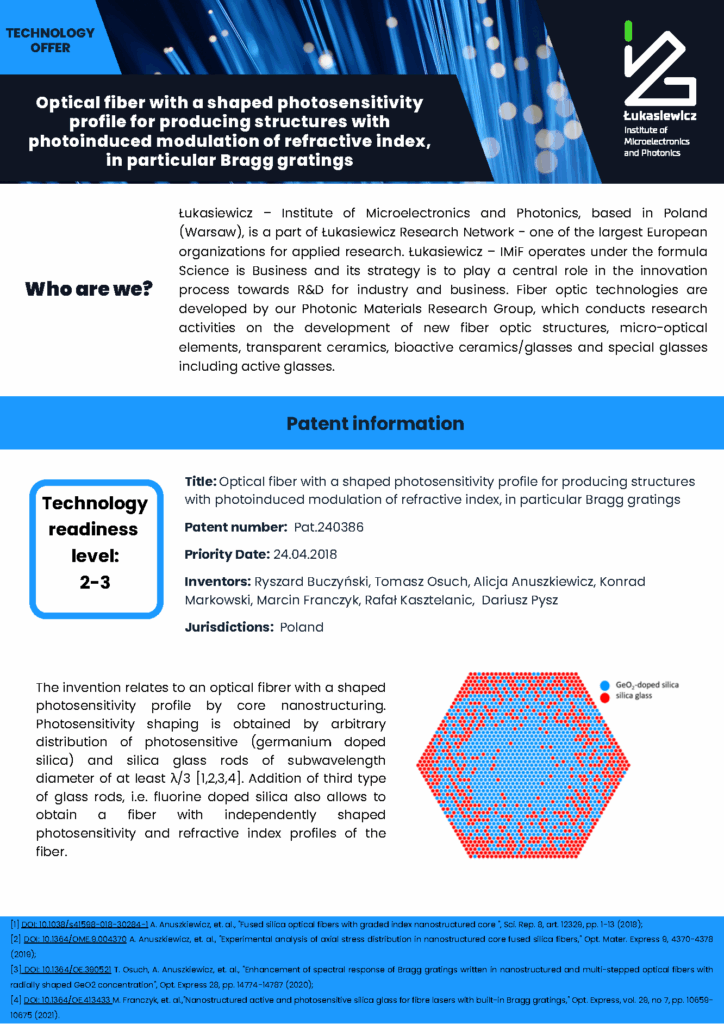
The invention relates to an optical fibrer with a shaped photosensitivity profile by core nanostructuring. Photosensitivity shaping is obtained by arbitrary distribution of photosensitive (germanium doped silica) and silica glass rods of subwavelength diameter of at least λ/3.
Addition of third type of glass rods, i.e. fluorine doped silica also allows to obtain a fiber with independently shaped photosensitivity and refractive index profiles of the fiber.
Patent information
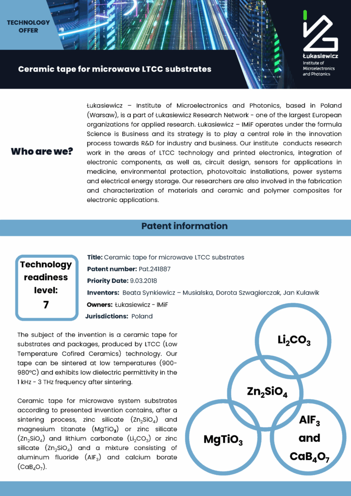
Title: Ceramic tape for microwave LTCC substrates
(PL: Taśma ceramiczna na mikrofalowe podłoża LTCC)
Patent number: Pat.241887
Application number: P.424833
Application date: 9.03.2018
Inventors: Beata Synkiewicz – Musialska, Dorota Szwagierczak, Jan Kulawik
Owner: Łukasiewicz – IMiF
Jurisdictions: Poland
The technology in a nutshell
The subject of the invention is a ceramic tape for substrates and packages, produced by LTCC (Low Temperature Cofired Ceramics) technology. Our tape can be sintered at low temperatures (900-980°C) and exhibits low dielectric permittivity in the 1 kHz – 3 THz frequency after sintering.
The ceramic tapes obtained according to the patent, show a low dielectric constant and a relatively low sintering temperature, making them a promising material for multilayer LTCC substrates for electronic circuits operating at very high frequencies. Thanks to our solution it can be possible to increase the speed of signal propagation, increase selectivity, reduce attenuation, and reduce power loss.
Patent information
Title: Positioning overlay
(PL: Nakładka pozycjonująca)
Utility model number: Ru.073237
Application number: W.129908
Application date: 10.03.2021
Inventors: Krzysztof Michalak, Joanna Branas, Lech Rządca,
Owner: Łukasiewicz – IMiF
Jurisdictions: Poland
UPRP: https://ewyszukiwarka.pue.uprp.gov.pl/search/pwp-details/W.129908
The technology in a nutshell
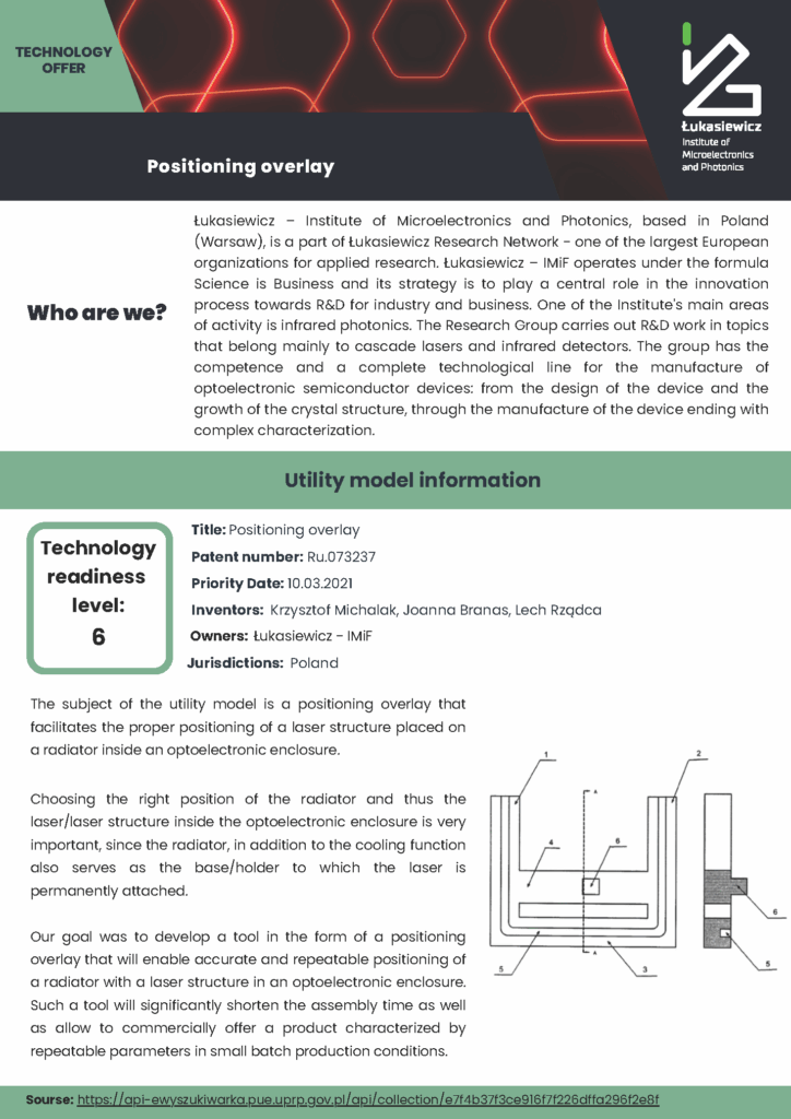
The subject of the utility model is a positioning overlay that facilitates the proper positioning of a laser structure placed on a radiator inside an optoelectronic enclosure.
Choosing the right position of the radiator and thus the laser/laser structure inside the optoelectronic enclosure is very important, since the radiator, in addition to the cooling function also serves as the base/holder to which the laser is permanently attached.
Our goal was to develop a tool in the form of a positioning overlay that will enable accurate and repeatable positioning of a radiator with a laser structure in an optoelectronic enclosure. Such a tool will significantly shorten the assembly time as well as allow to commercially offer a product characterized by repeatable parameters in small batch production conditions.
Patent information
Title: Centering frame
(PL: Ramka centrująca)
Utility model number: Ru.073236
Application number: W.129907
Application date: 10.03.2021
Inventors: Krzysztof Michalak, Joanna Branas, Lech Rządca,
Owner: Łukasiewicz – IMiF
Jurisdictions: Poland
UPRP: https://ewyszukiwarka.pue.uprp.gov.pl/search/pwp-details/W.129907
The technology in a nutshell
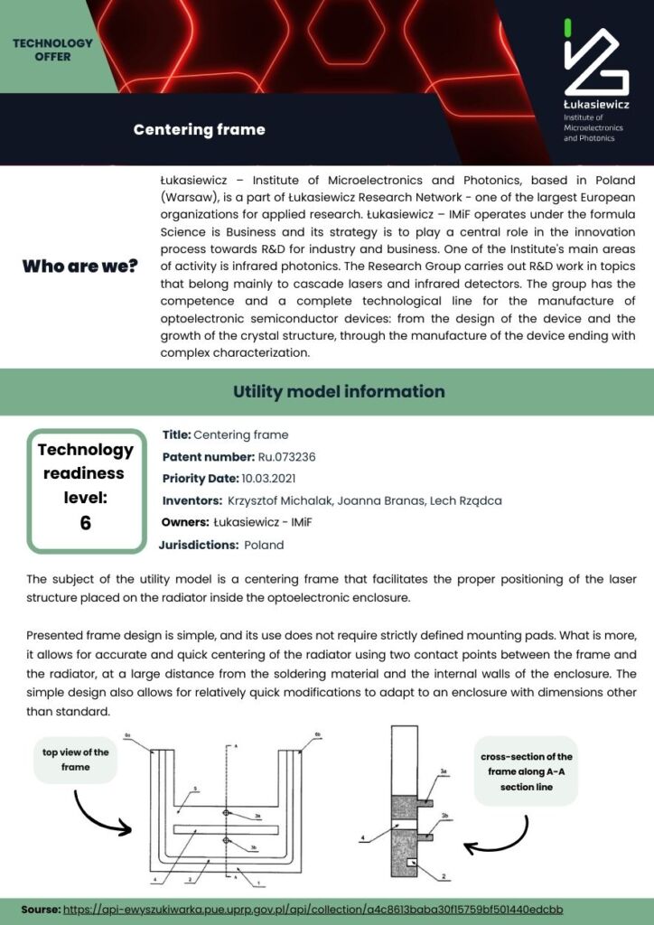
The subject of the utility model is a centering frame that facilitates the proper positioning of the laser structure placed on the radiator inside the optoelectronic enclosure.
Presented frame design is simple, and its use does not require strictly defined mounting pads. What is more, it allows for accurate and quick centering of the radiator using two contact points between the frame and the radiator, at a large distance from the soldering material and the internal walls of the enclosure. The simple design also allows for relatively quick modifications to adapt to an enclosure with dimensions other than standard.
This solution will both significantly shorten the required time and allow offering a product with repeatable parameters in commercial applications under small batch production conditions.
Method of producing gold-coated indium phosphide nanostructures and their use in surface-enhanced Raman scattering measurements
P.441658, EP23181729
Patent information
Title: Method of producing gold-coated indium phosphide nanostructures and their use in surface-enhanced Raman scattering measurements
(PL: Sposób wytwarzania nanostruktur InP pokrytych złotem i ich zastosowanie w pomiarach powierzchniowo-wzmocnionego rozpraszania ramanowskiego)
Patent number: –
Application number: P.441658, EP23181729
Application date: 6.07.2022 (PL), 27.06.2023 (EP)
Inventors: Jan Krajczewski, Andrzej Kudelski, Sylwia Turczyniak-Surdecka, Ewa Dumiszewska, Dariusz Czołak
Owners: Warsaw University, Łukasiewicz – IMiF
Jurisdictions: EPO, Poland
The technology in a nutshell
The object of the invention is a method of producing gold-coated InP nanostructures. Our method is mainly based on two steps the first of which is that, on a monocrystalline InP substrate, nanowires are grown using the method of metalorganic chemical vapour deposition, by introducing trimethylindium and phosphine in a constant manner into the reactor, wherein the carrier gas is hydrogen, wherein the ratio of the flow rate of phosphine to the flow rate of trimethylindium is no higher than 1000, wherein, during the introduction of trimethylindium and phosphine into the reactor, a constant temperature within a range of 370°C to 390°C and a pressure of 100 mbar are maintained. In the second step, the surface of the grown nanowires is coated with a gold layer by plasma spraying with a direct current of 20 mA. The object of the invention is also the use of gold-coated InP nanostructures as a platform for the measurements of surface-enhanced Raman scattering.
A method of manufacturing an active optical fibre and the active optical fibre
US10132993, EP3339261
Patent information
Title: A method of manufacturing an active optical fibre and the active optical fibre
(PL: Sposób wytwarzania światłowodu aktywnego i światłowód aktywny)
Patent number: US10132993, EP3339261
Application number: US201715852565, EP17208625
Application date: 22.12.2017 (US), 19.12.2017 (EP),
Inventors: Ryszard Buczyński, Dariusz Pysz, Marcin Franczyk, Mariusz Klimczak, Rafał Kasztelanic, Ryszard Stępień
Owner: Łukasiewicz – Institute of Microelectronic and Photonics
Jurisdictions: United States of America, France, Great Britain, Germany, Switzerland, Poland
Espacenet: https://worldwide.espacenet.com/patent/search/family/060674045/publication/EP3339261B1?q=EP3339261b1
The technology in a nutshell
The invention relates to a method of manufacturing an active optical fiber, called nanostructuring, in which the fiber core is composed of a few thousand subwavelength rods with similar diameters ordered in the hexagonal lattice. When the rods are made of two or more types of glasses with different refractive indices, their distribution determines the local refractive index experienced by a light beam.
Nanostructuring allows to obtain any gradient arbitrary refractive index profile if the size of a single nanostructured component is much smaller than the wavelength, i.e. λ/5. In active fiber, at least one type of glass is doped with rare earth (RE) ions.
Patent information
Title: Microprobe for selective electroporation and manufacturing method of such a microprobe
(PL: Mikrosonda do elektroporacji selektywnej i sposób wytwarzania takiej mikrosondy)
Patent number: US10322280, EP3011995, Pat.226157
Application number: US201515519444, EP15183159, P.409831
Application date: 21.10.2015 (US), 31.08.2015 (EP), 21.10.2014 (PL)
Inventors: Ryszard Buczynski, Dariusz Pysz, Ryszard Stępień
Owner: Łukasiewicz – Institute of Microelectronic and Photonics
Jurisdictions: United States of America, France, Great Britain, Germany, Switzerland, Poland
Espacenet: https://worldwide.espacenet.com/patent/search/family/054359701/publication/EP3011995B1?q=EP3011995b1
The technology in a nutshell
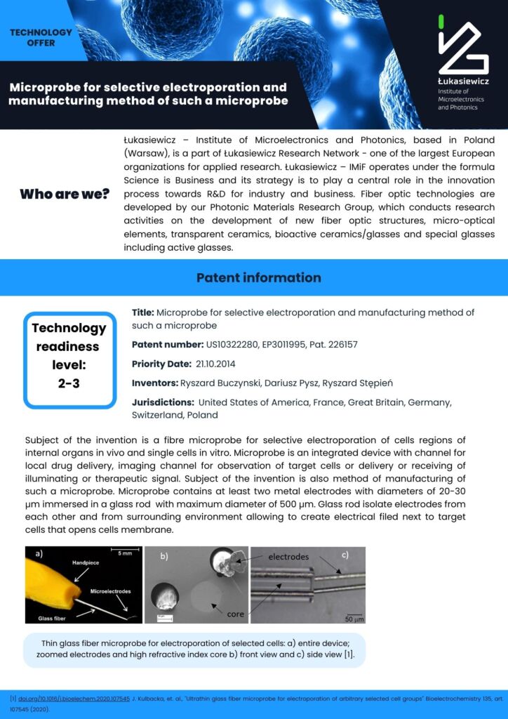
Subject of the invention is a fibre microprobe for selective electroporation of cells regions of internal organs in vivo and single cells in vitro. Microprobe is an integrated device with channel for local drug delivery, imaging channel for observation of target cells or delivery or receiving of illuminating or therapeutic signal. Subject of the invention is also method of manufacturing of such a microprobe.
Microprobe contains at least two metal electrodes with diameters of 20-30 μm immersed in a glass rod with maximum diameter of 500 μm. Glass rod isolate electrodes from each other and from surrounding environment allowing to create electrical filed next to target cells that opens cells membrane.