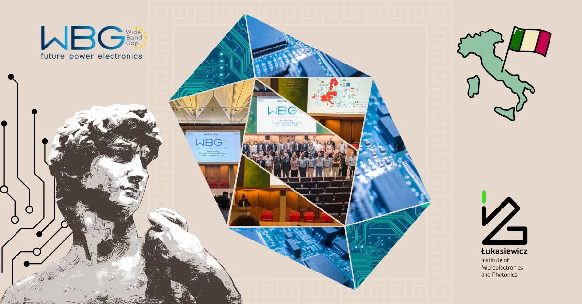
The project focuses on developing advanced semiconductor technologies with applications in key sectors such as industrial, automotive, renewable energy, consumer electronics and defence.
The project will launch the WBG Pilot Line (Wide Band Gap semiconductors pilot line), which will be one of four pilot lines funded by the European Union and Member States. The international consortium comprises 22 research units and universities from Italy, Sweden, Finland, Austria, Germany, France, and Poland.
The pilot line constitutes the development of innovative material and instrument technologies based on wide bandgap semiconductors such as gallium nitride (GaN), aluminum nitride (AlN), silicon carbide (SiC), and gallium oxide (Ga2O3). The Polish research and development units, Łukasiewicz – IMiF and IWC PAN, will be responsible for developing techniques for the growth of GaN substrates and epitaxial layers, as well as GaN and Ga2O3-based device manufacturing technologies.
Financing:
Consortium members:

Implementation
Total budget: ~360 mln € (50% contribution from UE/50% member states)
Project timeline (estimated): Q1 2025-Q4 2029 (60 months)

The project coordinator:
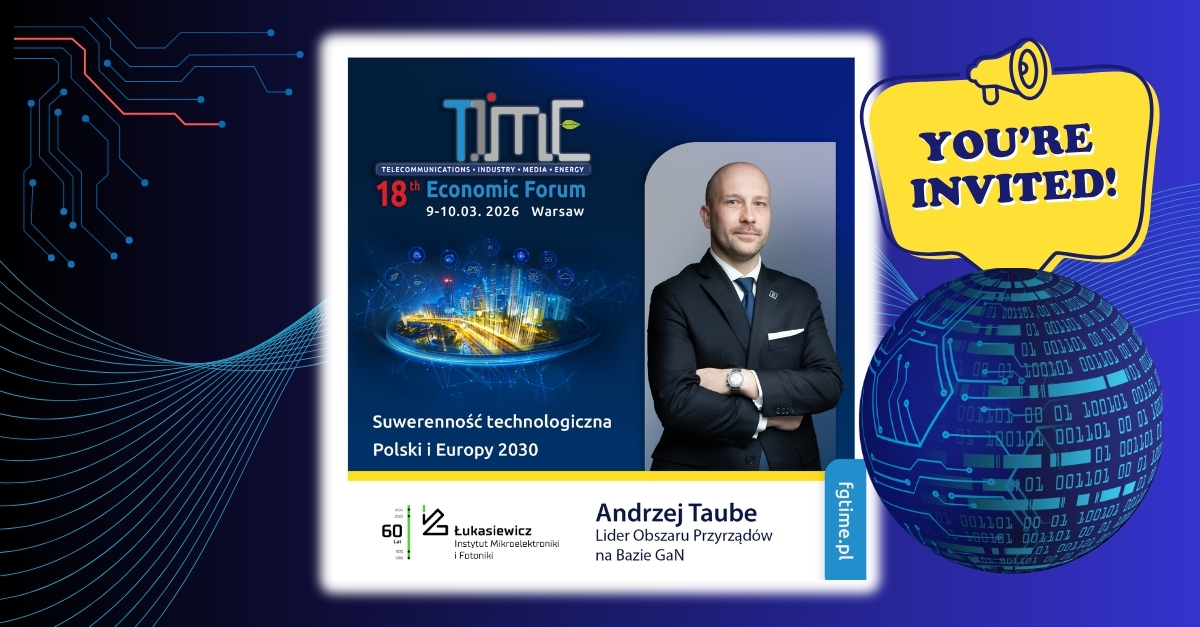
Andrzej Taube, PhD, Eng

Program
")

Zobacz zdjęcia